- 您现在的位置:买卖IC网 > Sheet目录511 > SI5040-D-GM (Silicon Laboratories Inc)IC TXRX XFP 10GBPS 32LGA
Si5040
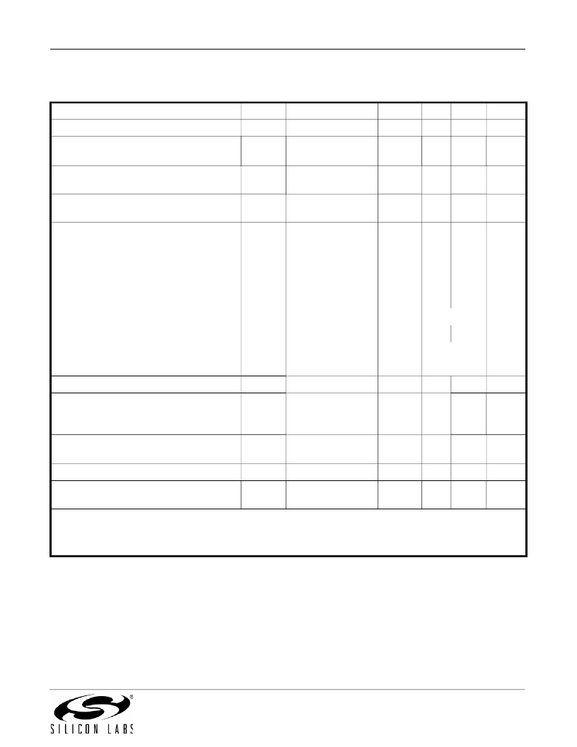
Table 5. AC Characteristics—TXDOUT (Transmitter Output)
(V DD = 1.8 V +5/–10%, T A = –40 to 95 ? C)
Parameter
Output Rise + Fall Times
Output Return Loss
Random RMS Jitter Generation,
TXDOUT 1
Total Peak-to-Peak Jitter
Generation, TXDOUT 1
Symbol
t R , t F
J GEN(rms)
J GEN(PP)
Test Condition
Figure 2
400 kHz–10 GHz
10 GHz–16 GHz
OC-192, CMU mode
0
OC-192, CMU mode
0
Min
20
6
4
—
—
Typ
25
—
—
2.8
36
Max
30
—
—
4.6
60
Unit
ps
dB
dB
mUI RMS
mUI PP
Jitter Transfer Bandwidth
(Programmable)
CMU bandwidth [3:0]
(Register 134, bits 7:4)
0000
—
180
220
Hz
0001
J BW
9.95 Gbps
—
1.37
1.76
kHz
0010
—
Not supported
kHz
0100
—
380
760
kHz
0101
0110
—
—
Not supported
Not supported
kHz
kHz
Jitter Transfer Peaking
< 120 kHz
—
0.03
dB
Acquisition Time
T AQ
REFCLK
Referenceless
—
—
—
—
50
61
ms
ms
Input Reference Clock Frequency 2
RC FREQ
ref clk /16 mode
618.75
622
709.4
MHz
ref clk /64 mode
154.687
155
177.35
Input Reference Clock Duty Cycle
Input Reference Clock Frequency
RC DUTY
RC TOL
40
–100
—
—
60
100
%
ppm
Tolerance
Notes:
1. PRBS31 or SONET framed PRBS31 data. The integrated CMU filters out SONET framing effects.
2. Input reference clock frequency can be either Baud rate/16 or Baud rate/64 ±100 ppm. The typical and maximum
numbers specified here correspond to /16 or /64 of the typical and maximum data rate that the device supports.
Rev. 1.3
11
发布紧急采购,3分钟左右您将得到回复。
相关PDF资料
SI5402DC-T1-GE3
MOSFET N-CH D-S 30V 1206-8
SI5403DC-T1-GE3
MOSFET P-CH 30V 6A 1206-8
SI5432DC-T1-GE3
MOSFET N-CH 20V 6A 1206-8
SI5440DC-T1-GE3
MOSFET N-CH D-S 30V 1206-8
SI5441DC-T1-GE3
MOSFET P-CH D-S 20V 1206-8
SI5443DC-T1-GE3
MOSFET P-CH D-S 20V 1206-8
SI5468DC-T1-GE3
MOSFET N-CH D-S 30V 1206-8
SI5475BDC-T1-GE3
MOSFET P-CH 12V 6A 1206-8
相关代理商/技术参数
SI5040-D-GMR
制造商:Silicon Laboratories Inc 功能描述:XFP Transceiver 1TX 1RX 10Gbps 32-Pin LGA T/R 制造商:Silicon Laboratories Inc 功能描述:XFP TRANSCEIVER, PB FREE - Tape and Reel 制造商:Silicon Laboratories Inc 功能描述:IC TXRX XFP 10GBPS 32LGA
SI5040-D-ZM2
制造商:Silicon Laboratories Inc 功能描述:XFP TRANSCEIVER, PB FREE - Rail/Tube
SI5040-D-ZM6
制造商:Silicon Laboratories Inc 功能描述:XFP TRANSCEIVER - Rail/Tube
SI5040-D-ZM7
制造商:Silicon Laboratories Inc 功能描述:XFP TRANSCEIVER, PB FREE - Rail/Tube
SI5040-EVB
功能描述:BOARD EVAL SI5040 RoHS:否 类别:编程器,开发系统 >> 评估演示板和套件 系列:- 产品培训模块:Obsolescence Mitigation Program 标准包装:1 系列:- 主要目的:电源管理,电池充电器 嵌入式:否 已用 IC / 零件:MAX8903A 主要属性:1 芯锂离子电池 次要属性:状态 LED 已供物品:板
SI5041-B-GM
制造商:Silicon Laboratories Inc 功能描述:10G DUAL CDR (REV B FOR PROTOTYPE ONLY, REV C FOR P - Rail/Tube
SI5041-B-GMR
制造商:Silicon Laboratories Inc 功能描述:10G DUAL CDR (REV B FOR PROTOTYPE ONLY, REV C FOR P - Tape and Reel
SI5041-C-GM
制造商:Silicon Laboratories Inc 功能描述:10G DUAL CDR, LEAD FREE - Rail/Tube
